

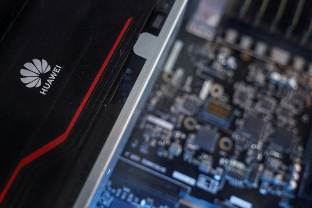
Huawei is signaling that the next leap in chip performance may come from redesigning how systems move data, not just from shrinking transistors. The company has outlined a target for high-end chips to reach transistor density comparable to a 1.4 nanometer process by 2031, even as it operates under heavy U.S. restrictions on advanced semiconductor technology.
A different route to performance
At a semiconductor symposium in Shanghai, Huawei introduced a new principle called Tau Scaling Law. The idea focuses on cutting the time it takes for signals and data to travel inside a chip and across a computing system.
That approach reflects a broader shift in thinking across the industry. Huawei is treating efficiency at the system level as the next major source of progress, rather than relying only on smaller transistor nodes.
He Hui, semiconductor research director at Omdia, described the move as a transition from traditional node-based scaling to system-level efficiency scaling. He said shorter interconnects, lower latency, and better data movement make sense at a time when leading-edge lithography is difficult to access.
An ambitious target from a wide technology gap
Huawei’s 1.4 nanometer target is striking because China’s most advanced proven chip manufacturing is still widely believed to be around the 7 nanometer level. By contrast, Taiwan Semiconductor Manufacturing Co. is already using 2 nanometer technology and plans to begin mass production of 1.4 nanometer chips in 2028.
Analysts say China is still unlikely to reach that level through conventional manufacturing alone. U.S. export restrictions have limited Chinese companies’ access to the most advanced chipmaking tools, especially the equipment needed for leading-edge nodes.
That makes Huawei’s new direction more than a technical statement. It is also a response to the reality that the classic race to smaller transistors has become harder to sustain under sanctions.
LogicFolding will start with phones, then expand
Huawei said the first product to use its Tau Scaling-based architecture, called LogicFolding, will be a Kirin phone launching later this year. The company says the design will shorten wiring paths inside the chip and deliver a meaningful performance improvement.
Huawei also plans to bring LogicFolding to Ascend chips in 2030. Beyond that, it expects the technology to be used in large AI clusters made up of hundreds or thousands of chips that support data centers.
The company added that its chip division has designed and mass-produced 381 chips over the past six years based on Tau Scaling Law. Those chips have been used across industries, including smartphones and AI computing.
Why the AI race matters
The strategic weight of Huawei’s chip roadmap is rising because of its role in China’s AI ecosystem. Huawei’s Ascend chips help power major Chinese AI models, including DeepSeek V4, which was released last month.
Demand for Ascend chips has also increased this year as domestic technology companies look for alternatives to Nvidia. Nvidia itself faces restrictions on selling its most advanced AI processors to China.
Nvidia CEO Jensen Huang said earlier this month that the company had “largely conceded” the China AI chip market to Huawei. That assessment shows how far Huawei’s influence has expanded beyond its own product line.
Recovery after sanctions
Huawei was placed on the U.S. trade blacklist in 2019, cutting off many of its links to American technology, including chips and software. The restrictions also made it harder for the company to depend on global contract chip manufacturers.
In response, Huawei entered an extreme survival mode. A secret backup chip project led by He Tingbo, who serves as president of Huawei’s semiconductor business and director of its Scientist Committee, became central to the company’s recovery effort.
The comeback became visible in 2023 with the Mate 60 series 5G phone, powered by a system-on-chip made by SMIC using 7 nanometer technology. SMIC shares rose 7.6% on Monday after Huawei’s LogicFolding announcement, while Huawei had also set up an advanced packaging research institute in Shanghai in January.
Technical hurdles remain
Even with the new architecture and the growing strategic importance of Ascend, Huawei still faces significant engineering challenges. Brady Wang of Counterpoint Research said cost, power, heat, and system integration remain major obstacles, especially for cloud AI servers.
He Hui also said Huawei’s latest approach still requires new chip design tools suited to Tau Scaling. He pointed to the challenge of controlling overheating in both smartphones and large-scale AI data center systems.