Huawei is signaling that it does not intend to wait for access to the most advanced manufacturing tools before pushing further into semiconductors. The company says it is aiming for transistor density comparable to a 1.4nm process by 2031, even as U.S. sanctions continue to limit its access to cutting-edge chip equipment.
The plan is built around a new design approach called LogicFolding. Huawei describes it as a move away from the traditional flat circuit layout and toward a vertically stacked structure that shortens wiring paths inside the chip and speeds up signal transfer.
A different path to denser chips
Huawei says LogicFolding is meant to expand circuit layout from a single layer to two layers. That change is intended to increase transistor density without relying on the same manufacturing route used by leading chipmakers with broader equipment access.
Alongside that idea, Huawei has introduced a guiding principle it calls Tau Scaling Law. Instead of focusing only on shrinking transistors, as in Moore’s Law, the new principle emphasizes reducing the time needed for signals and data to move through a chip and computing system.
He Tingbo, president of Huawei’s semiconductor business, presented the approach at the IEEE International Symposium on Circuits and Systems in Shanghai. The company says this shift reflects an effort to improve performance through architecture as much as through process scaling.
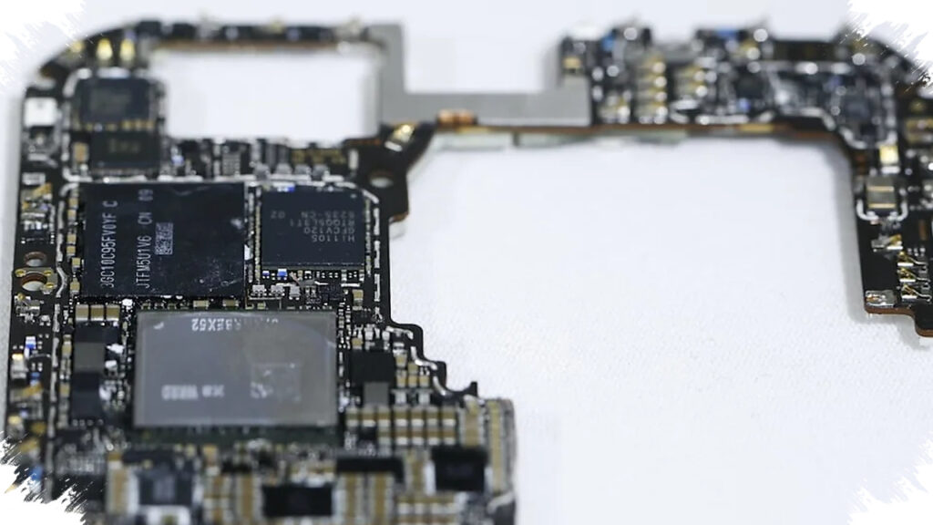
Commercial rollout begins with phones
Huawei says LogicFolding will first appear in a commercial smartphone chip, the Kirin, scheduled for the autumn 2026 season. After that, the same approach is planned for Ascend AI chips in 2030.
The company also says its chip division has brought 381 chips into mass production over the past six years since adopting Tau Scaling Law. That portfolio includes chips for smartphones and AI computing applications.
Technical limits remain
Huawei has also acknowledged that the path ahead is not straightforward. He Tingbo pointed to two major challenges: software tools for chip design are not yet ready for the new architecture, and heat dissipation becomes more difficult when components are stacked vertically.
“Given all the various constraints, we have found some pretty good solutions,” He Tingbo told Reuters. He added that Huawei’s solutions for mobile computing and AI computing will be competitive over the next 10 years.
Still, the company’s claims are attracting caution from analysts. Paul Triolo, head of technology at DGA Group, told CNBC that stacked designs can improve effective density, but that does not mean Huawei has solved the process, yield, power, thermal, and device performance issues associated with 1.4nm-class manufacturing.
Why the claim matters now
The announcement comes after years of pressure on Huawei following its addition to the U.S. trade blacklist in 2019. That move cut off access to many American technologies and pushed Huawei to search for a more independent development path.
The situation shifted in 2023 when the Mate 60 series arrived with a domestically made 5G system-on-chip. That chip was produced by Semiconductor Manufacturing International Corp on a 7nm node, and its appearance surprised many industry watchers who had doubted how far sanctions had constrained Huawei.
Reuters noted that Huawei’s latest claim has not been backed by third-party verification or independent benchmarking data. In semiconductors, production yield, power consumption, and thermal stability often determine whether a design is truly ready for broad use.
The gap with the global leaders remains large. Reuters reported that 7nm is still the highest node that domestic Chinese chipmakers have been able to demonstrate reliably, while TSMC is already running volume production at 2nm and is targeting mass production of 1.4nm in 2028, according to NBC News.
Huawei’s new architecture therefore places the company back at the center of the debate over China’s chip strategy. It is betting that design innovation can offset manufacturing limits, but the market is still waiting for proof that a density claim tied to 1.4nm can become a stable and efficient product.