Samsung Foundry and Cadence are widening their collaboration at a moment when AI workloads are pushing semiconductor design into a more demanding phase. The focus is no longer only on raw speed, but also on how efficiently a chip can be integrated, validated, and prepared for large-scale AI systems.
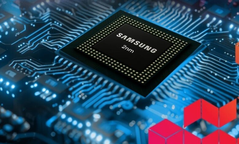
The partnership centers on second-generation 2nm chip development and more advanced 3D-IC designs. That combination is being positioned as a key foundation for next-generation AI processors built for data centers, HPC, robotics, autonomous vehicles, and smart devices.
A design push shaped by AI demand
The rapid rise of generative AI and physical AI is forcing the industry to move toward higher capacity, better power efficiency, and faster connectivity. Those requirements are driving Cadence and Samsung Foundry to optimize their design platform for Samsung’s second-generation 2nm manufacturing process.
The goal is to help customers accelerate development of next-generation AI and HPC systems without weakening design reliability. Boyd Phelps, Senior Vice President and General Manager of Cadence’s Silicon Solutions Group, said the industry is moving toward advanced nodes and 3D-IC, and that this shift demands greater capacity, stronger integration, and more validation confidence than before.
Samsung sees growing interest in 2nm
Samsung Foundry says interest in 2nm technology is increasing as AI use expands across more sectors. Jongshin Shin, Executive Vice President and Head of Foundry Design Platform Development at Samsung Electronics, described the second-generation 2nm node as one of the important foundations for future AI chips.
According to Shin, customers are showing stronger interest in Samsung Foundry’s second-generation 2nm technology for leading-edge AI designs. That demand is tied to AI infrastructure and physical AI applications, both of which require chips that can keep up with rising compute needs.
Samsung and Cadence are also building out a more mature semiconductor and 3D-IC platform. It is backed by advanced memory, high-speed interface IP, and workflows optimized specifically for AI.
NVIDIA adds strength to the ecosystem
The collaboration is also supported by NVIDIA through NVLink-C2C integration and CUDA-X GPU acceleration. Both technologies are important for high-speed data transfer between chips, which matters in large-scale AI systems.
Timothy Costa, Vice President and General Manager of Computing Engineering at NVIDIA, said modern design complexity requires tools that can keep pace with chip architecture development. He added that the semiconductor ecosystem depends on platforms that can match simulation and design requirements at advanced nodes.
NVIDIA also highlighted Cadence’s GPU-accelerated design flow on Samsung Foundry’s second-generation 2nm platform. Together, these capabilities are aimed at improving performance, enabling next-generation AI architectures, and supporting high-bandwidth interconnects.
Beyond data centers
The value of 2nm development is not limited to AI data centers. The same technology is also seen as relevant for fast-growing edge AI devices, including robotics, drones, autonomous machines, and intelligent sensor systems.
Ambarella is one company mentioned in connection with this direction, as it looks to use the technology for a next-generation edge AI platform based on the 2nm process. Chan Lee, Chief Operating Officer at Ambarella, said support from Cadence and Samsung Foundry is important for accelerating low-power AI innovation.
Lee said Ambarella’s edge AI strategy focuses on high performance per watt, scalable AI acceleration, and robust multi-sensor processing. He also noted that access to IP, design tools, and signoff-ready platforms helps speed development while reducing risk.
A broader shift in AI infrastructure
The long-term cooperation between Cadence and Samsung Foundry shows that AI chip competition is now about more than manufacturing speed. The industry is also pursuing more efficient designs, tighter integration, and platforms that can support large AI infrastructure.
With second-generation 2nm technology, 3D-IC design, advanced memory, high-speed interfaces, and NVIDIA ecosystem support, the next phase of AI chip development is becoming more complete. That shift could translate into stronger performance for future data centers, robotics, autonomous vehicles, and smart devices.