

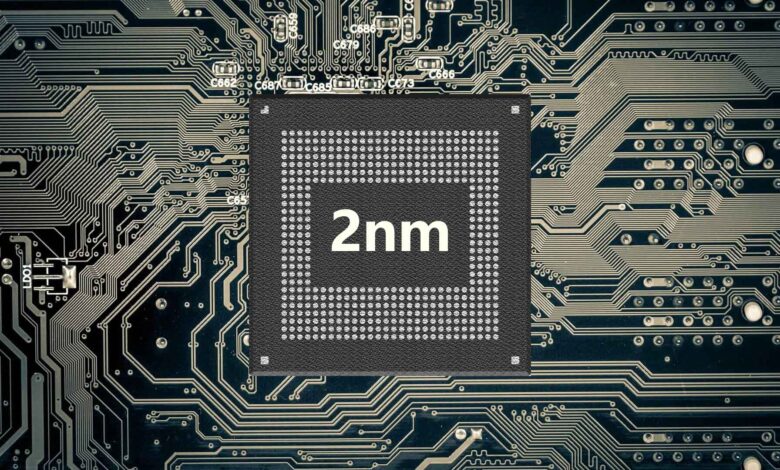
Samsung is taking a different route for its next 2nm chips by bringing design and manufacturing optimization together from the start. The shift is meant to balance transistor scaling with chip size, cost, power efficiency, performance, and yield in one connected process.
The company laid out the strategy at SAFE Forum 2026 at Samsung Electronics’ headquarters in Seocho, South Korea. There, Samsung Foundry made clear that 2nm development is no longer being treated as separate design and fabrication work.
DTCO becomes the core approach
Samsung says it is using Design Technology Co-Optimization, or DTCO, to align chip architecture and process technology at the same time. That approach is becoming more important as semiconductor production gets more complex at smaller nodes.
For Samsung, the benefit is a better compromise between technical goals and business constraints that often pull in different directions. One of the biggest focus areas is SRAM, the ultra-fast memory embedded in processors and especially important for AI workloads.
Why SRAM matters for AI chips
SRAM is central to workloads that need instant access to data while keeping power use under control. In 2nm-era chips, improving SRAM can become a meaningful advantage for customers building AI and high-performance computing products.
That focus fits the broader direction of Samsung’s foundry business, where efficiency and speed are now just as important as raw scaling. The company appears to be positioning 2nm not only as a smaller node, but as a more practical one for demanding real-world chips.
| Area | Samsung’s focus | Why it matters |
|---|---|---|
| DTCO | Design and process are optimized together | Aims to improve balance between cost, performance, and yield |
| SRAM | Special attention for embedded high-speed memory | Supports AI and HPC workloads that need rapid data access |
| 2nm node | Co-designed from the earliest stages | Helps customers prepare more efficiently for next-generation chips |
A wider ecosystem backs the plan
Samsung says it is working with more than 21 partner companies across EDA, IP blocks, and other chip design technologies. More than 400 representatives from those 21 partner firms attended SAFE Forum 2026 and showcased tools built to support customers using Samsung Foundry’s process technology.
The scale of that participation shows how dependent advanced-node development has become on the surrounding ecosystem. Software, IP libraries, and verification tools all need to line up early so customers can move into production with fewer barriers.
AI demand is shaping the message
Samsung is also tying the effort to growing demand for AI chips and stronger partnerships with global AI firms, high-performance computing players, and South Korea’s semiconductor industry. The company wants to strengthen its role as a central part of the AI semiconductor ecosystem.
At a time when competition is intense, access to an advanced process is no longer enough on its own. Samsung is trying to build a broader path that includes design support, partner tooling, and examples of successful deployments.
One of those examples came from Rebellions, a South Korean AI accelerator startup. It presented a case study showing how Samsung’s ecosystem helped develop the Rebel100 NPU on Samsung Foundry’s 4nm process.
The Rebel100 is said to deliver 1,024 TFLOPs while consuming 600W, and it also uses Samsung’s HBM3E memory. The example was used to show how tightly linked technologies inside one ecosystem can support AI products.
Support for smaller fabless companies
Samsung is also working with South Korea’s Ministry of Trade, Industry and Energy on initiatives such as the M.AX Alliance and K-CHIPS project. Those programs are designed to develop AI semiconductor talent and support local fabless chip companies.
For smaller firms, the biggest challenge is often not the idea itself but the cost of turning a design into a prototype. That is where Multi-Project Wafer, or MPW, becomes important.
| Program | Purpose | Benefit |
|---|---|---|
| M.AX Alliance | Develop AI semiconductor talent | Helps strengthen the local ecosystem |
| K-CHIPS | Support fabless chip companies | Reduces early-stage development barriers |
| MPW | Shared wafer prototyping | Lets multiple firms test designs at lower cost |
MPW lets several companies test prototypes on a single shared production wafer, which can significantly reduce development costs before mass production begins. For startups and smaller fabless players, that can lower the barrier to trying a design on Samsung’s manufacturing process.
Samsung’s message from SAFE Forum 2026 is clear: the competition at 2nm is no longer only about what happens inside the fab. It is also about who can build the strongest design ecosystem, speed up AI adoption, and offer the easiest path for customers moving into the next generation.