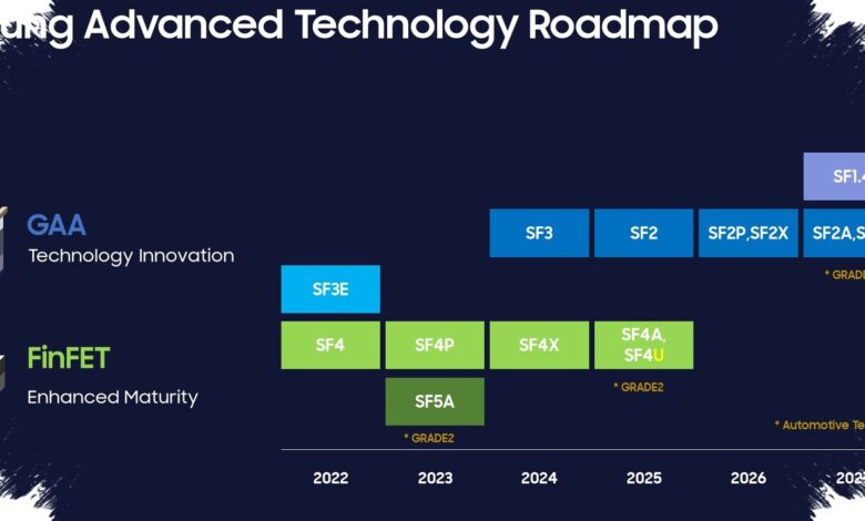
Samsung is bringing its 1.4nm chip project back to the forefront, a move that signals a fresh push in the race for the most advanced semiconductor nodes. The company has shifted its mass-production target for SF1.4 from 2027 to 2029 as it focuses on stabilizing the technologies already in use.
2nm progress is now shaping the next step
That change in direction follows Samsung’s decision to strengthen its 2nm lines first, including SF2 and SF2P, before committing more heavily to 1.4nm. The strategy appears to be paying off, with the company reportedly achieving high production success rates in 2nm and securing a major contract for Tesla’s next-generation AI chips.
The stronger position in 2nm has given Samsung more confidence to move SF1.4 back into priority planning. Rather than racing ahead on several fronts at once, the company is now trying to build a firmer foundation for the next node.
Competition is already waiting at 1.4nm
Samsung is not entering the 1.4nm field early. TSMC and Intel are already ahead at this level, with TSMC using the A14 name and Intel calling its version Intel 14A.
Intel plans to begin mass production at 1.4nm in 2027, while TSMC is targeting full production a year later. That timing suggests Samsung could trail its two main rivals by one to two years unless its execution improves quickly.
Even so, Samsung still has a potential advantage in how it prepares its manufacturing base. One of its key moves is faster adoption of next-generation lithography equipment than TSMC.
High-NA EUV is becoming a key weapon
ASML has reportedly delivered its High-NA Extreme Ultraviolet, or EUV, system to Samsung’s NRD-K facility. The equipment is expected to be used for printing special layers in the 1.4nm fabrication process.
Samsung is also working with major equipment suppliers in parallel, including Applied Materials and Lam Research. Both U.S. companies have been asked to begin early development of manufacturing tools for SF1.4.
Those first-wave machines are expected to go directly to NRD-K, Samsung’s most advanced semiconductor research and development center. That gives the company a more prepared test environment as it develops the new node.
Memory is moving forward too
Samsung’s semiconductor roadmap is not limited to logic chips. The company has also reportedly ordered new equipment to develop V12 NAND memory, which is intended as a future-generation storage technology.
That memory platform is projected to enter full-scale production around 2030. Together with the revived 1.4nm effort, it shows Samsung is preparing multiple layers of its business at once, from leading-edge logic to next-generation storage.
For Samsung, the return of SF1.4 is about more than chasing a smaller number on paper. It reflects a broader effort to stay competitive in a market where the speed of adopting the most advanced production tools may decide who leads next.