TSMC is pushing its 2nm rollout at a pace the company says is faster than any previous node transition. With demand for AI and high-performance computing chips still climbing sharply, the foundry is preparing a capacity expansion that is expected to outpace the growth seen during the 3nm ramp.
The scale of that move is notable because 2nm output is projected to rise by as much as 45% compared with capacity at the same stage of 3nm development. TSMC has also already said the 2nm process has entered mass production, which means the expansion is now tied to active manufacturing rather than preparation.
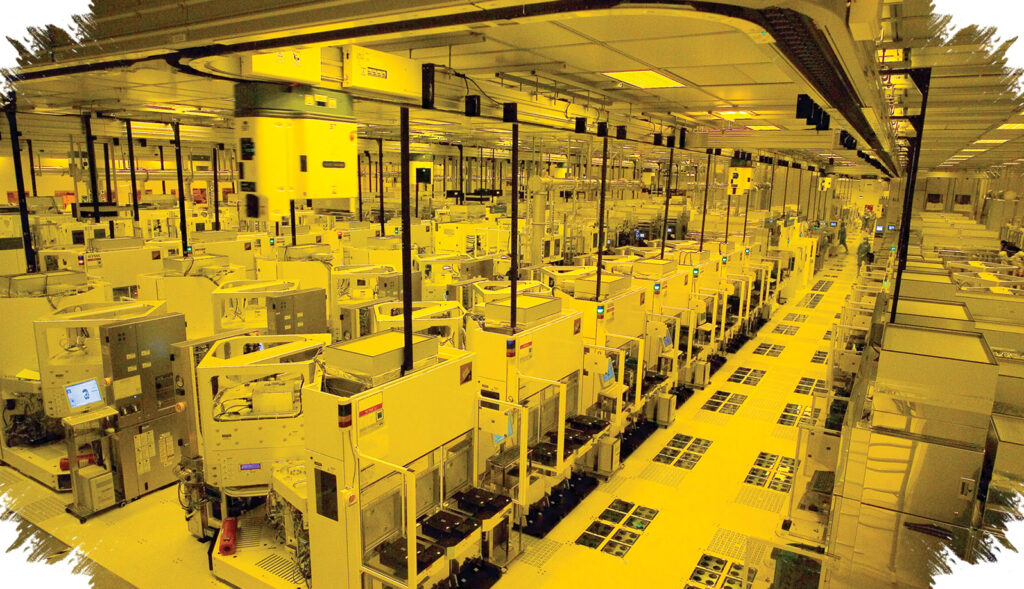
Five fabs are moving at once
At the Technology Symposium 2026 in Silicon Valley, TSMC Senior Vice President, Deputy Co-COO, and Chief Information Security Officer Hou Yung-ching said the company is advancing its expansion plan at “two times the speed.” He also said the yield learning curve for 2nm is better than it was for 3nm.
That point matters because 2nm uses a more complex nanosheet architecture. Even with that added complexity, TSMC says production is improving faster and strengthening its position at the frontier of advanced chip manufacturing.
Hou added that there has never been a year in which so many fabs introduced a new process at the same time. With five 2nm fabs ramping together, this transition stands apart from earlier node shifts.
AI demand is driving the urgency
The main reason behind the accelerated buildout is the surge in demand for AI and HPC chips. TSMC says wafer shipments for AI accelerators have increased 11 times, while demand for large chips using advanced packaging has risen 6 times.
That growth means extra capacity will not necessarily erase supply tightness right away. Even with more output coming online, high-performance chip supply is still expected to remain constrained because demand is rising so quickly.
A number of major customers are also reported to have secured large allocations of N2 capacity. NVIDIA, Apple, Qualcomm, and AMD are among the companies said to have booked meaningful portions of the early supply.
Apple is said to have secured more than half of TSMC’s initial N2 capacity. If accurate, that would underline how intense the competition is for access to the new node before full-scale capacity becomes available.
Expansion is broader than new fabs
TSMC is not relying only on new 2nm facilities to increase output. The company also plans to add or upgrade nine new plants and capacity-expansion projects each year, effectively doubling its historical expansion pace.
That effort is being reinforced by higher production at existing facilities as well. TSMC is also expanding manufacturing in Arizona in the United States, Kumamoto in Japan, and Dresden in Germany.
The company’s strategy therefore extends beyond one region or one new node. It is building a wider manufacturing base to support long-term demand from global customers.
Packaging has become part of the bottleneck
The race is not limited to wafer production. Demand for large chips with advanced packaging is also climbing, and TSMC is responding by accelerating investment in advanced packaging lines.
The company says ongoing improvements in 3D packaging technology have cut the time needed to reach mass production of SoIC chips by 75%. That helps speed up chip production when customers need increasingly complex designs.
Overall advanced packaging capacity is expected to grow 80% in 2027. That forecast matters because the semiconductor industry’s bottleneck is no longer only at wafer fabrication, but also in the advanced packaging stage required for top-end AI chips.
Taken together, the 2nm expansion and the faster packaging rollout show how TSMC is shaping its next phase of growth. The company is not only chasing smaller process nodes, but also building a fuller production path for the next generation of AI hardware.