

IBM has drawn fresh attention from the semiconductor industry by claiming a breakthrough that could reshape the next generation of PCs and smartphones. The company says it has built the world’s first sub-1nm chip technology, a milestone that points to faster devices, better energy efficiency, and stronger support for AI workloads.
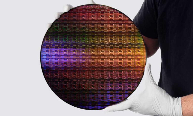
The prototype uses 0.7nm transistors, or 7 angstroms, and IBM says it can pack nearly 100 billion transistors into an area about the size of a fingernail. That density is almost twice as high as the early 2nm chip IBM introduced in 2021.
A new stack, not just smaller transistors
The key to the advance is an architecture IBM calls “nanostack.” Instead of laying transistors out in a flat pattern, the approach stacks and arranges them in 3D, creating a design that resembles a small, layered city.
This structure is intended to do more than increase transistor count. IBM says it also allows chip designers to mix materials in ways that improve performance and efficiency from each transistor, while supporting higher bandwidth for AI tasks.
Why device users may care
IBM estimates the sub-1nm chip could deliver up to 50 percent better performance and 70 percent better energy efficiency than its 2nm chip. In practical terms, that could mean more computing power and longer battery life without increasing processor size.
The actual benefit, however, would still depend on the final chip design and the workload running on it. Even so, semiconductor history shows that process gains often lead to major performance jumps before larger architecture changes arrive.
Industry leaders have followed a similar pattern before. Intel long used a “tick tock” strategy to alternate between new fabrication technology and new architecture, while Apple has previously claimed an edge over Intel and AMD in part by adopting newer manufacturing techniques earlier.
Not ready for consumer products yet
IBM has made clear that this chip is not a finished product for sale. The company expects the first sub-1nm chips could enter production within five years.
IBM also sees a longer runway for the technology. It projects at least another decade of development with nanostack, suggesting the path toward denser chips is still far from over.
Why the timing matters in the AI era
The strategic value of this kind of chip is greatest in AI. Large language models are known to be highly power-hungry, to the point that some governments have limited or banned new data center construction.
With higher efficiency, IBM’s approach could help reduce electricity use for AI workloads or enable more computing at the same energy level. That makes it relevant not only for servers, but also for PCs and smartphones that are increasingly expected to run AI features on-device.
IBM’s position in a crowded race
IBM’s announcement comes as the industry is only beginning to move into the 2nm era. The first 2nm chips to reach production this year include Samsung’s Exynos 2600, along with a new wave of Apple chips expected to include the A20 Pro and M6.
Intel is also pushing forward with Core Series 3 on the 18A process, or 1.8nm. Against that backdrop, IBM’s claim signals that chip scaling still has room to advance, even if consumer devices will need more time before those gains arrive.